domingo, 25 de julio de 2010

Optical Heterodyne Detection

Heterodyne detection (also called coherent detection) is a detection method which was originally developed in the field of radio waves and microwaves. There, a weak input signal is mixed with some strong "local oscillator" wave in some nonlinear device such as a rectifier, and the resulting mixing product is then detected, often after filtering out the original signal and the local oscillator frequency. The frequency of the mixing product is the sum or the difference of the frequencies of the signal and the local oscillator.

optical heterodyne setup
Figure 1: Setup for optical heterodyne detection.
Optical heterodyne detection involves optical signal and local oscillator waves, whereas the mixing product is an electrical signal. The mixing product is not obtained by mixing the signal and local oscillator wave in a nonlinear crystal, but rather simply by detecting the superimposed waves with a square-law photodetector, typically a photodiode. For example, one uses a beam combiner (or beam splitter) as in Figure 1 and aligns the two beams such that they are mode-matched. This means that their wavefronts have the same curvature on the detector, and the interference conditions are uniform over the full detector area. Of course, this is possible only if the two beams are spatially coherent. In a fiber-optic setup, a fiber coupler would be used instead of the beam splitter, and all fibers would be single-mode fibers, possibly of polarization-maintaining type.
The resulting photocurrent is proportional to the total optical intensity, thus to the square of the total electric field amplitude. If the signal and local oscillator powers and frequencies are constant, the photocurrent has two different frequency components:
  • The constant (zero-frequency) part is proportional to the sum of local oscillator and signal power.
  • The part oscillating with the difference frequency (the beat note) has an amplitude proportional to the product of the electric field amplitudes of signal and local oscillator.
The oscillating part can then be isolated and processed further with electronic means. Its electric power is proportional to the product of the powers of signal and local oscillator.
With a strong local oscillator, the heterodyne signal resulting from a weak input signal can be much more powerful than for direct detection. In this sense, heterodyne detection provides a signal gain, although there is no optical amplification involved.

Noise Limitations

The noise in the detected signal has different contributions:
  • There is shot noise, the power spectral density (PSD) of which is proportional to the optical average power.
  • The photodetector may add some noise, for example due to some dark current.
  • Additional noise can be added by the electronics.
In many cases, the local oscillator power is made so high that the corresponding shot noise PSD exceeds that of any other noise. The possible signal-to-noise ratio is then fundamentally limited by shot noise. It can be calculated from the ratio of mean squared photocurrent contributions:
signal-to-noise ratio for optical heterodyne detection
where Ps and Plo are the optical signal power and local oscillator, respectively, at the photodiode, ηq is the photodiode's quantum efficiency, ηm is the overlap factor for the two beams, and B is the detection bandwidth. This result equals the number of photoelectrons generated on average within a time 1 / B.
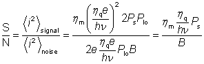
Further increases of local oscillator power would not increase the signal-to-noise ratio, as the signal power and the shot noise PSD are equally increased.
It is also apparent that the beam combiner (see Figure 1) should have a high transmission, so that most of the signal power is sent to the detector. The resulting high loss of local oscillator power at the detector can be compensated by increasing the local oscillator power incident on the beam splitter.
If the beam combiner's transmission is high and the beam overlap is good (ηq ∼ 1), the obtained signal-to-noise ratio is twice that for direct detection. In practice, heterodyne detection can offer a much greater advantage in terms of sensitivity, because direct detection reaches the shot noise limit only for rather high signal powers, whereas with heterodyne detection the standard quantum limit can be reached for much lower signal powers. Note, however, that there are cases where the standard quantum limit can not be reached because detector saturation limits the local oscillator power.
An important detail is that the measured signal is not at zero frequency, but rather at some finite difference frequency, where the detector noise (e.g., 1 / f noise) can be much weaker than around zero frequency.
Using an amplitude-squeezed local oscillator beam, it is even possible to beat the standard quantum limit with heterodyne detection.

Spatial Single-mode Nature of Heterodyne Detection

A strong heterodyne signal is obtained only if the beam overlap factor ηm is high. If the local oscillator beam is a perfect Gaussian beam, one may consider the total incident input signal light as a superposition of modes, using the mode system which is defined by the local oscillator beam. We see then that only the signal light in the lowest-order mode (the Gaussian) contributes to the heterodyne signal, because the overlap factors are zero for all higher-order modes. For any such higher-order mode, interference still occurs on the photodiode, but the local oscillations of intensity cancel out by integrating the power over the full detector area, provided that the detection efficiency is uniform over the full beam area.
The single-mode nature of heterodyne detection is a crucial aspect. It can be very helpful, for example by suppressing influences of stray light in sensitive measurements. On the other hand, it would greatly reduce the detection efficiency, for example when light scattered on a large area needs to be detected.
In principle, one could use a local oscillator beam consisting of different spatial modes, ideally each one being associated with a separate optical frequency. That would allow to simultaneously and independently measure signals in multiple modes. However, the power of each signal component in the heterodyne signal would then be proportional to the local oscillator power in the corresponding mode, whereas the noise level would be determined by the total local oscillator power. This shows again that heterodyne detection is essentially a single-mode detection technique.

Balanced Detection

balanced optical heterodyne setup
Figure 2: Setup for balanced optical heterodyne detection.
A remaining problem of heterodyne detection in the simple form as shown in Figure 1 is that excess noise of the local oscillator wave directly affects the signal. This is avoided with a balanced heterodyne setup [2, 6] as shown in Figure 2. Here, the beam splitter must have a reflectivity of precisely 50%. With a simple electronic circuit, one can obtain the difference of the two photocurrents. That difference is to first order not influenced by noise of the local oscillator.

Temporal Coherence Issues

If the laser delivering the local oscillator beam is totally independent of the signal, it is hardly possible to measure the phase of the input signal, because the phase of the electronic signal is also dependent on the local oscillator phase, which is stable only over the typically short coherence time.
If phase measurements are required, the local oscillator and signal waves are usually generated from a single source, so that the relative phase of the two beams is fairly stable even if the source does not exhibit particularly low phase noise. For example, a signal wave may be generated from a local oscillator wave by frequency-shifting part of it with an acousto-optic modulator. A heterodyne measurement can then very sensitively reveal any phase changes to that signal.
By bandpass-filtering the electronic signal, it is also possible to sample a very narrow spectral portion of the signal. That detection bandwidth can easily be far below what is possible with optical bandpass filters. This can be useful for precision spectroscopy, for example.

Homodyne Detection

A variant of heterodyne detection is homodyne detection, where the local oscillator frequency equals the signal frequency. For optical homodyne measurements, both waves are virtually always derived from the same laser source. The homodyne technique is phase-sensitive in the sense that the power of the heterodyne signal depends on the relative phase of signal and local oscillator, and may even totally vanish.
A useful modification is balanced homodyne detection, where two photodiodes (Figure 2) are used after a beam splitter with precisely 50% reflectivity, and the sum and difference of photocurrents are electronically obtained. If the signal port is blocked, the difference of photocurrents exhibits the shot noise level of the local oscillator beam, even if the actual noise level of that beam is different. The latter noise level can be obtained in addition by taking the sum of the photocurrents. That sum exhibits the same noise as for direct detection of the local oscillator beam with a single photodiode. The homodyne setup provides the difference signal in addition, which allows one to conveniently compare the actual noise with the shot noise limit. For amplitude-squeezed light, the sum of the photocurrents exhibits a lower noise than the difference. In many squeezed-light experiments, the degree of squeezing is measured with the homodyne technique.
A possible interpretation of the situation without signal input is that the setup then measures vacuum noise. This is because although no photons can enter the signal input port, there are still vacuum fluctuations of the electric field. The measured local oscillator shot noise is interpreted as being caused not by the local oscillator beam, but rather by the vacuum noise [5]. This interpretation is supported by the fact that amplitude-squeezed light at the signal input can reduce that noise level. These findings are in conflict with the earlier (and still widespread) idea that shot noise is intrinsic to the detection process rather than a property of the light field.

Heterodyne Measurements with Pulsed Beams

The heterodyne technique can also be applied to pulsed signals by using a pulsed local oscillator beam. It is even possible to use ultrashort pulses. As the heterodyne detector is essentially sensitive only while the local oscillator light is there (assuming a signal power well below the local oscillator power), it is possible to obtain a very high temporal resolution without requiring a very fast photodetector. This technique is called heterodyne (or homodyne) linear optical sampling.

Applications of Heterodyne Detection

Some examples for the application of optical heterodyne detection are:
  • Heterodyne detection is used for coherent Doppler LIDAR measurements (and related laser radar techniques), where very weak light scattered in the atmosphere needs to be detected. It is possible, for example, to accurately measure wind speeds based on the Doppler shift. By deriving the signal and local oscillator beams from the same laser source (see above), it is possible to resolve very small Doppler shifts.
  • There are other applications in spectroscopy. Examples are solar radiometry [3] and cavity ring-down spectroscopy [13].
  • The linewidth of a laser, for example, can be measured with the self-heterodyne technique, where a frequency-shifted copy of the laser beam is superimposed with a temporally delayed copy on a photodetector.
  • In optical fiber communications, the phase sensitivity of heterodyne and homodyne detection allows one to demodulate phase-encoded signals [7, 9], based on techniques like frequency shift keying (FSK) (→ coherent communications). Also, it the basis for some forms of electronic dispersion compensation.

Ricardo Monroy   C.I. 17646658


Electro-optic Modulators


An electro-optic modulator (EOM) (or electrooptic modulator) is a device which can be used for controlling the power, phase or polarization of a laser beam with an electrical control signal. It typically contains one or two Pockels cells, and possibly additional optical elements such as polarizers. Different types of Pockels cells are shown in Figure 1 and are described more in detail in the article on Pockels cells. The principle of operation is based on the linear electro-optic effect (also called the Pockels effect), i.e., the modification of the refractive index of a nonlinear crystal by an electric field in proportion to the field strength. Frequently used nonlinear crystal materials for EOMs are potassium di-deuterium phosphate (KD*P = DKDP), potassium titanyl phosphate (KTP), beta-barium borate (BBO) (the latter for higher average powers and/or higher switching frequencies), also lithium niobate (LiNbO3), lithium tantalate (LiTaO3) and ammonium dihydrogen phosphate (NH4H2PO4, ADP). In addition to these inorganic electro-optic materials, there are also special polymers for modulators.
Pockels cells
Figure 1: Pockels cells of various types.
The voltage required for inducing a phase change of π is called the half-wave voltage (Vπ). For a Pockels cell, it is usually hundreds or even thousands of volts, so that a high-voltage amplifier is required. Suitable electronic circuits can switch such large voltages within a few nanoseconds, allowing the use of EOMs as fast optical switches. In other cases, a modulation with smaller voltages is sufficient, e.g. when only a small amplitude or phase modulation is required.

Types of Electro-optic Modulators

Phase Modulators

The simplest type of electro-optic modulator is a phase modulator containing only a Pockels cell, where an electric field (applied to the crystal via electrodes) changes the phase delay of a laser beam sent through the crystal. The polarization of the input beam often has to be aligned with one of the optical axes of the crystal, so that the polarization state is not changed.
Many applications require only a small (periodic or nonperiodic) phase modulation. For example, this is often the case when one uses an EOM for monitoring and stabilizing a resonance frequency of an optical resonator. Resonant modulators (see below) are often used when a periodic modulation is sufficient, and make possible a large modulation depth with a moderate drive voltage. The modulation depth can in some cases be so high that dozens of sidebands are generated in the optical spectrum (comb generators, frequency combs).

Polarization Modulators

Depending on the type and orientation of the nonlinear crystal, and on the direction of the applied electric field, the phase delay can depend on the polarization direction. A Pockels cell can thus be seen as a voltage-controlled waveplate, and it can be used for modulating the polarization state. For a linear input polarization (often oriented at 45° to the crystal axes), the output polarization will in general be elliptical, rather than simply a linear polarization state with a rotated direction.

Amplitude Modulators

Combined with other optical elements, in particular with polarizers, Pockels cells can be used for other kinds of modulation. In particular, an amplitude modulator (Figure 2) is based on a Pockels cell for modifying the polarization state and a polarizer for subsequently converting this into a change in transmitted optical amplitude and power.
electro-optic amplitude modulator
Figure 2: Electro-optic amplitude modulator, containing a Pockels cell between two polarizers.
An alternative technical approach is to use an electro-optic phase modulator in one arm of a Mach-Zehnder interferometer in order to obtain amplitude modulation. This principle is often used in integrated optics (for photonic integrated circuits), where the required phase stability is much more easily achieved than with bulk optical elements.
Optical switches are modulators where the transmission is either switched on or off, rather than varied gradually. Such a switch can be used, e.g., as a pulse picker, selecting certain pulses from a train of ultrashort pulses, or in cavity-dumped lasers (with an EOM as cavity dumper) and regenerative amplifiers.

Thermally Compensated Devices

In configurations where the induced relative phase change between two polarization directions is used, thermal influences can be disturbing. Therefore, electro-optic modulators often contain two matched Pockels cells in an athermal configuration where the temperature dependence of the relative phase shift is largely canceled. There are also configurations with four crystals of exactly the same length, canceling both birefringence effects and spatial walk-off. Various types of multi-crystal designs are used, depending on the material and the exact requirements.

Resonant Versus Broadband Devices

For some applications, a purely sinusoidal modulation with constant frequency is required. In that case, it is often beneficial to use an electrically (not mechanically) resonant electro-optic modulator, containing a resonant LC circuit. The input voltage of the device can then be substantially lower than the voltage across the electrodes of the Pockels cell. A high ratio of these voltages requires a high Q factor of the LC circuit and reduces the bandwidth in which strong resonant enhancement can be achieved. The disadvantage of using a resonant device is that one loses flexibility: changing the resonance frequency requires the exchange of at least one electric component.
Broadband modulators are optimized for operation in a wide frequency range, which typically starts at zero frequency. A high modulation bandwidth typically requires a Pockels cell with a small electric capacitance, and excludes the exploitation of a resonance.

Traveling-Wave Modulators

For particularly high modulation bandwidths e.g. in the gigahertz region, integrated optical traveling-wave modulators are often used. Here, the electric drive signal generates an electromagnetic wave (microwave) propagating along the electrodes in the direction of the optical beam. Ideally, the phase velocities of both waves are matched so that efficient modulation is possible even for frequencies which are so high that the electrode length corresponds to several wavelengths of the microwave.

Important Properties

A number of properties should be considered before purchasing an electro-optic modulator:
  • The device must have a sufficiently large open aperture, particularly in cases with high peak powers. A high crystal quality and appropriate electrode geometry are required for uniform switching or modulation across the full open aperture. The price can significantly rise for increasing aperture sizes.
  • For switching ultrashort pulses, effects of Kerr nonlinearity and chromatic dispersion may be relevant, which depend on the crystal material and length and also on the beam radius. (Significant effects of this kind often cannot be avoided and thus have to be taken into account in the design of, e.g., a regenerative amplifier.)
  • Depending on the device design, the polarization of the incoming beam may or may not be maintained in the output.
  • A phase modulator may generate unwanted amplitude modulation, and vice versa. This depends strongly on the design.
  • As electro-optic materials are also piezo-electric, the applied voltage can introduce mechanical vibrations, which themselves can affect the refractive index via the elasto-optic effect. Around certain mechanical resonance frequencies, the modulator response may be strongly modified. This can be a problem particularly for broadband modulators. In switching applications, unwanted ringing effects can occur. Such effects depend strongly on the crystal material, dimensions, orientation and mechanical design.
  • Both high optical average powers and high switching frequencies can induce thermal problems. The thermal handling and thus the power and frequency capabilities depend on various construction details.
  • The crystal(s) should have high-quality anti-reflection coatings, designed for the required range of operation wavelengths, and of course a good material transparency, in order to minimize the insertion losses.
  • Rejected optical beams may be absorbed within the modulator device, or (particularly for high-power devices) leave the device at a more or less convenient location and direction.
  • The switching speed (rise time, fall time) depends on properties of both the modulator (e.g. via its capacitance) and the electronic driver.
  • Electro-optic modulators can be purchased in fiber-coupled form, with different types of connectors and fibers (e.g. single-mode or multimode).
Note that a proper mechanical mount is also required, often with means to align the modulator precisely in various directions.

Electronic Driver

It is important to use an electronic driver which is both well matched to the EOM and suitable for the particular application. For example, different kinds of EOMs require different drive voltages, and the driver should also be designed for the given electrical capacitance of the EOM. Some drivers are suitable for a purely sinusoidal modulation, whereas broadband devices work in a large range of modulation frequencies. Many problems can be avoided by purchasing an electro-optic modulator together with the electronic driver from the same supplier, because the responsibility for the overall performance is then at one place.

Applications

Some typical applications of electro-optic modulators are:

Ricardo Monroy   C.I. 17646658


Acousto-optic modulator


An acousto-optic modulator (AOM), also called a Bragg cell, uses the acousto-optic effect to diffract and shift the frequency of light using sound waves (usually at radio-frequency). They are used in lasers for Q-switching, telecommunications for signal modulation, and in spectroscopy for frequency control. A piezoelectric transducer is attached to a material such as glass. An oscillating electric signal drives the transducer to vibrate, which creates sound waves in the glass. These can be thought of as moving periodic planes of expansion and compression that change the index of refraction. Incoming light scatters (see Brillouin scattering) off the resulting periodic index modulation and interference occurs similar to in Bragg diffraction. The interaction can be thought of as four-wave mixing between phonons and photons. The properties of the light exiting the AOM can be controlled in five ways:


An acousto-optic modulator consists of a piezoelectric transducer which creates sound waves in a material like glass or quartz. A light beam is diffracted into several orders. By vibrating the material with a pure sinusoid and tilting the AOM so the light is reflected from the flat sound waves into the first diffraction order, up to 90% deflection efficiency can be achieved.
Deflection
A diffracted beam emerges at an angle θ that depends on the wavelength of the light λ relative to the wavelength of the sound Λ
\sin\theta = \left (\frac{ m\lambda}{2\Lambda} \right)
in the Bragg regime and
\sin\theta = \left (\frac{ m\lambda_0}{n\Lambda} \right)
with the light : normal to the sound waves, where m = ..., −2, −1, 0, 1, 2, ... is the order of diffraction. Diffraction from a sinusoidal modulation in a thin crystal solely results in the m = −1, 0, +1 diffraction orders. Cascaded diffraction in medium thickness crystals leads to higher orders of diffraction. In thick crystals with weak modulation, only phasematched orders are diffracted, this is called Bragg diffraction. The angular deflection can range from 1 to 5000 beam widths (the number of resolvable spots). Consequently, the deflection is typically limited to tens of milliradians.

Intensity


The amount of light diffracted by the sound wave depends on the intensity of the sound. Hence, the intensity of the sound can be used to modulate the intensity of the light in the diffracted beam. Typically, the intensity that is diffracted into m = 0 order can be varied between 15% to 99% of the input light intensity. Likewise, the intensity of the m = 1 order can be varied between 0% and 80%.
Frequency
One difference from Bragg diffraction is that the light is scattering from moving planes. A consequence of this is the frequency of the diffracted beam f in order m will be Doppler-shifted by an amount equal to the frequency of the sound wave F.
f \rightarrow f + mF
This frequency shift is also required by the fact that energy and momentum (of the photons and phonons) are conserved in the process. A typical frequency shift varies from 27 MHz, for a less-expensive AOM, to 400 MHz, for a state-of-the-art commercial device. In some AOMs, two acoustic waves travel in opposite directions in the material, creating a standing wave. Diffraction from the standing wave does not shift the frequency of the diffracted light.
Phase
In addition, the phase of the diffracted beam will also be shifted by the phase of the sound wave. The phase can be changed by an arbitrary amount.
Polarization
Collinear transverse acoustic waves or perpendicular longitudinal waves can change the polarization. The acoustic waves induce a birefringent phase-shift, much like in a Pockels cell. The acousto-optic tunable filter, especially the dazzler, which can generate variable pulse shapes, is based on this principle[1].
Acousto-optic modulators are much faster than typical mechanical devices such as tiltable mirrors. The time it takes an AOM to shift the exiting beam in is roughly limited to the transit time of the sound wave across the beam (typically 5 to 100 nanoseconds). This is fast enough to create active modelocking in an ultrafast laser. When faster control is necessary electro-optic modulators are used. However, these require very high voltages (e.g. 10 kilovolts), whereas AOMs offer more deflection range, simple design, and low power consumption (less than 3 watts).


Ricardo Monroy   C.I. 17646658


Acousto-Optic Modulators

A different approach to modulator technology uses the interaction between light and sound waves to produce changes in optical intensity, phase, frequency, and direction of propagation. Acousto-optic modulators are based on the diffraction of light by a column of sound in a suitable interaction medium.
When a sound wave travels through a transparent material, it causes periodic variations of the index of refraction. The sound wave can be considered as a series of compressions and rarefactions moving through the material. In regions where the sound pressure is high, the material is compressed slightly. This compression leads to an increase in the index of refraction. The increase is small, but it can produce large cumulative effects on a light wave passing some distance through the compressed material.
An acousto-optic device requires a material with good acoustic and optical properties and high optical transmission. Several types of material are available. We shall describe acoustic-optic materials in more detail later.
The sound wave is produced by a piezoelectric transducer. Piezoelectric materials exhibit slight changes in physical size when voltage is applied to them. An example of one such material is crystalline quartz. If the piezoelectric material is placed in contact with the acousto-optic material and a high-frequency oscillating voltage is applied to the piezoelectric material, it will expand and contract as the voltage varies. This in turn exerts pressure on the acousto-optic material and will launch an acoustic wave (sound wave) which will travel through the material. The frequency F of the acoustic wave will be the same as the frequency of the applied voltage. The acoustic wave will have a wavelength L given by:
FL = C Equation 3
where C is the velocity of sound in the material, typically of the order of 105 cm/sec. Variation of the acoustic frequency of the driver will thus change the acoustic wavelength, which in turn changes the characteristics of the acousto-optic interaction.
A typical structure for an acousto-optic device is shown in Figure 5. The piezoelectric materials and metal layers are bonded or deposited on the acousto-optic material. A radio-frequency field is applied across the piezoelectric material using the metal layers as electrodes. The acoustic wave is then launched into the acousto-optic medium by the piezoelectric material. Acoustic waves propagating from a flat piezoelectric transducer into a crystal will form almost plane wavefronts traveling in the crystal. The opposite end of the material from the transducer should have an acoustic termination to suppress reflected acoustic waves.
7_fig5.jpg (16981 bytes)
Fig. 5
Typical structure of an acousto-optic device
The elasto-optic properties of the medium respond to the acoustic wave so as to produce a periodic variation of the index of refraction. A light beam incident on this disturbance is partially deflected in much the same way that light is deflected by a diffraction grating. The operation is shown in Figure 6. The alternate compressions and rarefactions associated with the sound wave form a grating that diffracts the incident light beam. No light is deflected unless the acoustic wave is present.
7_fig6.jpg (20442 bytes)
Fig. 6
Diagram showing the principles of operation of an acousto-optic light-beam modulator or deflector. The diagram defines the Bragg angle F and deflection angle F used in the text.
For a material with a fixed acoustic velocity, the acoustic wavelength or grating spacing is a function of the radio-frequency drive signal; the acoustic wavelength controls the angle of deflection. The amplitude of the disturbance, a function of the radio-frequency power applied to the transducer, controls the fraction of the light that is deflected. Thus, the power to the transducer controls the intensity of the deflected light. Modulation of the light beam is achieved by maintaining a constant radio frequency, allowing only the deflected beam to emerge from the modulator and modulating the power to the transducer. Thus the modulator will be in its off state when no acoustic power is applied and will be switched to its transmissive state by the presence of acoustic power.
The transmission T of an acousto-optic modulator is
T = T0 sin2(p (M2PL/2H)0.5/l cos Q ) Equation 4
where P is the acoustic power supplied to the medium, l is the wavelength, L is the length of the medium (length of the region in which the light wave interacts with the acoustic wave), H is the width of the medium (width across which the sound wave travels), and the inherent transmission T0 is a function of reflective and absorptive losses in the device. The quantity M2 is a figure of merit, a material parameter that indicates the suitability of a particular material for this application. It is defined by
M2 = n6p2/r v3 Equation 5
where p is the photoelastic constant of the material, r is its density, and v is the velocity of sound in the material. This figure of merit relates the diffraction efficiency to the acoustic power for a given device. It is useful for specifying materials to yield high efficiency, but in practical devices, bandwidth is also important, so that specifying a high value of M2 alone is not sufficient.
The angle Q is the so-called Bragg angle. The diffraction of the light beam by the periodic array of acoustic waves satisfies the same relationship as the scattering of X rays by periodic planes of atoms (so-called Bragg scattering). Hence the diffraction of the light waves is also referred to as Bragg reflection. Bragg reflection of X rays occurs at the planes of atoms in a crystal which are spaced a regular distance apart. The so-called Bragg angle gives the angle at which the most efficient reflection occurs. The phenomenon of optical reflection from the regular wavefronts of the acoustic waves is exactly the same, with the provision that the acoustic wavelength replaces the distance between planes of atoms.
The Bragg angle Q is defined as the angle the beam makes with the reflecting waves. It is given by:
sin Q = l /2nL Equation 6
where n is the index of refraction of the material, l is the optical wavelength and L is the acoustic wavelength.
To use the acousto-optic device as a modulator, one should employ the deflected beam as shown in Figure 7. This will give higher values of the extinction ratio than using the undeflected beam. When the acoustic drive is off, the light in the direction of the deflected beam is zero. When the acoustic drive is on, light is diffracted into that direction. Thus, the acousto-optic device controls the light in that direction, turning it on and off at will. The device is operated as a modulator by keeping the acoustic wavelength (frequency) fixed and varying the drive power to vary the amount of light in the deflected beam. As we shall see later, the use as a light-beam deflector is somewhat different.
7_fig7.jpg (17497 bytes)
Fig. 7
Use of an acousto-optic device as a light-beam modulator
The design and performance of acousto-optic beam modulators have several limitations. The transducer and acousto-optic medium must be carefully designed to provide maximum light intensity in a single diffracted beam, when the modulator is in an open condition. The transit time of the acoustic beam across the diameter of the light beam imposes a limitation on the rise time of the switching and therefore limits the modulation bandwidth. The acoustic wave travels with a finite velocity and the light beam cannot be switched fully on or fully off until the acoustic wave has traveled all the way across the light beam. Therefore, to increase bandwidth, one focuses the light beam to a small diameter at the position of the interaction so as to minimize the transit time. Frequently the diameter to which the beam may be focused is the ultimate limitation for the bandwidth. If the laser beam has high power, it cannot be focused in the acousto-optic medium without damage.
General Comments of John Simcik
The rise time tr for an acousto-optic modulator is given by the equation:
tr = d/C Equation 7
where d is the diameter of the laser beam in the region of the interaction and C is the velocity of sound in the material. As an example, for a tellurium dioxide acousto-optic modulator, with an acoustic velocity of 8.03 � 105 cm/sec and a laser-beam diameter of 100 m m, the rise time is 0.01 cm/8.03 � 105 cm/sec = 1.245 � 10- 8 = 12.45 nsec. Thus acousto-optic devices are capable of high-frequency modulation.
Acousto-optic light-beam modulators have a number of important desirable features. The electrical power required to excite the acoustic wave may be small, less than one watt in some cases. High extinction ratios are obtained easily because no light emerges in the direction of the diffracted beam when the device is off. A large fraction, up to 90% for some commercial models, of the incident light may be diffracted into the transmitted beam. Acousto-optic devices may be compact and may offer an advantage for systems where size and weight are important. As compared to electro-optic modulators, they tend to have lower bandwidth, but do not require high voltage.
Table 2 presents the characteristics of some materials used in commercially available acousto-optic modulators. Several materials are available for use in the visible and near-infrared regions, and one material (germanium) is useful in the far infrared. The table also presents some values for the figure of merit M2, at a wavelength of 633 nm, except for GaAs (1530 nm) and Ge (10.6 mm). The factors that enter into the definition of M2 vary with crystalline orientation; the values in the table are for crystals oriented to maximize M2. The values for bandwidth and for typical drive power are representative of commercially available acousto-optic devices.


Ricardo Monroy  C.I. 17646658


Electro-Optic Modulators


In this section, we discuss the operation and application of electro-optic devices that rely on the phenomenon of birefringence that is induced by application of voltage to a crystal. Let us first define birefringence. In certain crystalline materials, an incident light ray will separate into two rays that may travel in different directions. These crystals are called birefringent. The direction in which the light travels is dependent on its polarization. For each of the two different perpendicular states of polarization, the light will travel in a different direction. Birefringence is also called double refraction because when the light enters the crystal, it is refracted into two different directions.
Figure 1 shows the effect of birefringence when a beam of unpolarized light enters the surface of a birefringent material at an angle q to the normal to the surface. The two different components of polarization (horizontal and vertical) travel in two different directions. The material has two different indices of refraction, one for each of the two perpendicular components of polarization. In accordance with the laws of geometric optics, the two rays are refracted at different angles as they enter the crystal.

7_fig1.jpg (20941 bytes)

Fig. 1
Schematic diagram showing the separation of the two
components of polarization in a light beam traveling through a
birefringent material. The incident light is unpolarized.

Many crystalline materials exhibit birefringence naturally, without application of any voltage. The birefringence is present all the time. Examples of such crystals are quartz and calcite.
There are also a number of crystals that are not birefringent naturally but in which application of a voltage induces birefringence. This phenomenon is called the electro-optic effect. The electro-optic effect leads to the ability to control light beams in a variety of ways and is the basis of a number of applications, including light-beam modulators, Q-switches, and deflectors. Examples of crystals that exhibit the electro-optic effect are potassium dihydrogen phosphate (commonly called KDP), ammonium dihydrogen phosphate (ADP), potassium dideuterium phosphate (KD*P), lithium niobate, and barium sodium niobate.
The operation of an electro-optic device used as a light-beam modulator is shown schematically in Figure 2. Polarized light is incident on the modulator. The light may be polarized originally or a polarizer may be inserted, as shown. The analyzer, oriented at 90� to the polarizer, prevents any light from being transmitted when no voltage is applied to the electro-optic material. When the correct voltage is applied to the device, the direction of the polarization is rotated by 90� . Then the light will pass through the analyzer.

7_fig2.jpg (20543 bytes)

Fig. 2
Schematic diagram of the operation of a modulator based
on the electro-optic effect. In this configuration, the voltage is
applied parallel to the direction of light propagation.

Two types of electro-optic effect have been used: the Kerr electro-optic effect, which is shown by liquids such as nitrobenzene, and the Pockels electro-optic effect, shown by crystalline materials such as ammonium dihydrogen phosphate or lithium niobate. Some early electro-optic devices used nitrobenzene, but the liquid tends to polymerize in the presence of the intense laser light. Modern electro-optic modulators use the Pockels effect. The electro-optic modulators are often called Pockels cells.
The orientation of the polarizer and analyzer at 45� to the vertical, as shown in Figure 1, is a common configuration, used with many commercial modulators. But the orientation depends on the particular material used and on the direction in which the crystal has been cut. The manufacturer's instructions should be consulted to ensure proper orientation of the modulator and the directions of the pass axes for the polarizer and analyzer.
With the direction of polarization at 45� to the vertical direction, the polarization vector is composed of two perpendicular components of equal intensity, one vertical and one horizontal. The crystalline element is oriented with its axes in a specified orientation (which depends on the crystalline symmetry of the particular material). The applied voltage induces birefringence in the crystal, so that the two components of polarization travel with different velocities inside the crystal. This induced birefringence is the basis of the electro-optic effect.
The two components travel in the same direction through the crystal and do not become physically separated. But the two components, in phase as they enter the crystal, emerge with different phases. As they traverse the crystal, they accumulate a phase difference, which depends on the distance traveled and on the applied voltage. When the beams emerge from the crystal, the polarization of the combined single beam depends on the accumulated phase difference. If the phase difference is one-half wavelength, the polarization is rotated by 90� from its original direction. This by itself does not change the intensity of the beam. But, with the analyzer, the transmission of the entire system varies, according to

T = T0 sin2(p D nL/l ) Equation 1
where T is the transmission, T0 the intrinsic transmission of the assembly, taking into account all the losses, D n the birefringence (that is, the difference in refractive index for the two polarizations), L the length of the crystal, and l the wavelength of the light. The birefringence is an increasing function of the applied voltage, so that the transmission of the device will be an oscillatory function of applied voltage. The maximum transmission occurs when
D n = l /2L Equation 2
This occurs at a voltage called the half-wave voltage, denoted V1/2. The half-wave voltage depends on the nature of the electro-optic material. The half-wave voltage for a particular material increases with the wavelength. Thus, in the infrared the required voltage is higher than in the visible. This factor can limit the application of electro-optic modulators in the infrared.
The transmission of an electro-optic device as a function of applied voltage is shown in Figure 3, indicating the maximum transmission at the half-wave voltage.

7_fig3.jpg (19072 bytes)

Fig. 3
Transmission of an electro-optic device as a function of applied voltage.
V1/2 denotes the half-wave voltage.

In most crystals, each of the prominent crystalline faces belongs to one of three families of planes that intersect along what are called crystal axes. These axes can be designated as coordinate axes, even though they are not generally at right angles to each other. When one fabricates an electro-optic modulator, the crystal must be cut at certain specified angles to the crystalline axes. A full discussion of the different orientations and the reasons for them is beyond the scope of this module. We simply note that different crystalline symmetries require that specific relations be maintained between the crystalline axes and the faces of the electro-optic element.
One important performance parameter for electro-optic modulators is the extinction ratio, defined as the ratio of the transmission when the device is fully open, to the transmission when the device is fully closed. In practice there is always some light leakage, so the minimum transmission never reaches zero. A high value of the extinction ratio is desirable because it determines the maximum contrast that may be obtained in a system that uses the modulator. Commercial electro-optic modulators can have extinction ratios in excess of 1000.
Electro-optic modulators may be fabricated with different physical forms. In one form, voltage is applied parallel to the light propagation, as was shown in Figure 2. One uses transparent electrodes or electrodes with central apertures. This is called a longitudinal electro-optic modulator.
In another form, metal electrodes are on the sides of the crystal (which has a square cross section) and the voltage is perpendicular to the light propagation. This is called a transverse modulator. Two examples are shown in Figure 4. The top is a two-element configuration suitable for use with materials like ADP. The use of two crystals oriented as shown provides compensation for the natural birefringence of the material. The bottom portion of the figure shows a single-element configuration suitable for lithium tantalate-type materials. Both single- and dual-element configurations are in use in commercial modulators.

7_fig4.jpg (20778 bytes)

Fig. 4
Transverse electro-optic modulator configurations.
Top: Two-element configuration suitable for ADP-type materials.
Bottom: Single-element configuration suitable for lithium tantalate-type materials

Longitudinal and transverse modulators have different applications. Longitudinal modulators may have large apertures, but the half-wave voltage will be high, often in the kilovolt range. Longitudinal modulators are often used with conventional light sources. Because it is difficult to vary the required high voltages rapidly, the frequency response of longitudinal modulators tends to be low. Applications for which longitudinal modulators are suited include relatively low-frequency modulation of laser beams or use with non-laser sources.
In transverse modulators, the voltage is applied perpendicular to the light propagation. The phase retardation for a given applied voltage may be increased simply by making the crystal longer. The half-wave voltage thus may be much lower for transverse modulators, perhaps as low as 100 volts. It follows that the frequency response may be much higher. Transverse modulators are thus suited for fast, broadband applications. A problem with transverse modulators is the relatively small aperture that they permit, because the crystal may be a long, thin parallelepiped. This physical configuration means that transverse modulators are best suited for use with narrow, well-defined laser beams. In addition, the extinction ratios available with transverse modulators tend to be lower than for longitudinal modulators. Applications of transverse modulators include broadband optical communication, display and printing systems, and fast image and signal recorders.
Table 1 lists electro-optic materials and some of their characteristics. The table includes the names of a number of electro-optic materials, their common abbreviations, their chemical formulas, and the spectral range over which they are transmissive. The bandwidths quoted are for use of the materials in commercially available electro-optic light modulators. Most of the materials are suited for use in the visible and near-infrared portions of the spectrum, but cadmium telluride is useful as a modulator for CO2 lasers in the long-wavelength infrared.
Of the materials in the table, ADP, AD*P, and KD*P are relatively older materials. They may be used as either longitudinal or transverse modulator materials, but have relatively high half-wave voltages.
Lithium niobate and lithium tantalate represent a relatively modern class of electro-optic materials, which have larger electro-optic effects and smaller half-wave voltages. They are hard to grow in large crystals of high quality but they are perhaps the best available modern electro-optic materials.


Ricardo Monroy  C.I. 17646658


SINGLE-PHOTON SOURCES

Quantum dots may hold the key to secure quantum cryptography

Much as the laser dramatically changed the telecommunications industry and led to rapid scientific progress in many fields, a single-photon source (SPS) would push photonics to its fundamental limit—control of single quanta—and lead to major advances. While many of those advances are not immediately obvious, there are even now three uses for an SPS.
First among these uses is in quantum cryptography, which promises unconditionally secure communications.1 Second, an SPS could also be applied to quantum computation following the ingenious scheme of Knill, Laflamme, and Milburn, which requires only a source of indistinguishable single photons, high-efficiency photon detectors, and linear optical elements to carry out such tasks as Shor's algorithm for factoring large numbers in finite time and Grover's algorithm for searching an unordered database (see www.laserfocusworld.com/articles/355975).2 These algorithms promise to speed up difficult computational problems. Third, an emerging application of an SPS is to drive a different system such as an atom or even a mechanical oscillator.
While these applications, primarily the first two, are driving development of SPSs across institutions, researchers will certainly find abundant unforeseen uses for these sources.


There have been several proposed sources of single photons and many proof-of-principle demonstrations in many systems. These systems fall into four rough categories. The first two categories are based on attenuated laser pulses and spontaneous parametric downconversion in nonlinear crystals, respectively.
While much research has been put into developing these sources and even implementing them in cryptography schemes, they both suffer from the fact that the emission is inherently classical and composed of a broad distribution of photon numbers, which leads to a non-negligible number of multiphoton events, reducing the level of security in a quantum cryptography scheme. In practice, these events can be reduced by further attenuation, but only at the cost of a reduced bit-rate.
The third category of SPSs uses a collective excitation of a cold, atomic vapor. This technique produces highly indistinguishable photons, but is difficult to implement because it requires trapping and cooling of the atoms, in addition to multiple-pulse laser preparation sequences. The probabilistic nature of creating the excitation, as well as the lack of optical confinement, has limited the largest single-photon rate to 100 s.1
The fourth category of SPS is based on a single quantum emitter like an atom, molecule, defect color center, or quantum dot. These sources rely on the fact that when these optically active emitters are excited, they decay primarily by the emission of a single photon. A wide range of these types of sources have been demonstrated, including single molecules, single atoms trapped in cavities, single self-assembled quantum dots, single nitrogen-vacancy centers in diamond, and recently single carbon nanotubes.3
The primary limitation and difficulty in working with these systems is the ability to observe and collect emission from a single emitter. Typically, this task is performed in condensed matter systems with microphotoluminescence (PL) spectroscopy, which uses a combination of spectral filtering and confocal microscopy techniques to eliminate emission from nearby emitters (see Fig. 1, left). The emission is then analyzed using a Hanbury-Brown and Twiss (HBT) interferometer to verify single-photon emission (see Fig. 1, right).

Quantum dots take the lead

Self-assembled quantum dots (QDs) have emerged as a very attractive candidate because of the ease of incorporating them into existing optoelectronic semiconductor technology. In addition, QDs have a near-perfect quantum efficiency and fast, 1 ns radiative lifetime at low temperature. Quantum dots can also be excited nonresonantly by carrier relaxation from nearby quantum wells or from the bandgap of the host semiconductor. Proof of single-photon emission in QDs was first demonstrated in 2000 using a low density of cadmium selenide (CdSe) quantum dots on a glass substrate and since then the field has progressed rapidly. The most commonly used system is composed of indium arsenide (InAs) QDs embedded in a gallium arsenide (GaAs) matrix.

Microcavities benefit QDs

Advances in nanofabrication techniques have led to development of various semiconductor microcavities such as micropillars, microdisks, and 2-D photonic-crystal defect cavities. Embedding the QDs inside a microcavity offers four important and interrelated benefits for their use as single-photon sources. First, the cavity size limits the number of QDs that can participate and effectively acts as a spatial filter that is at least equal to, if not better, than the diffraction-limited spot achieved by a good microscope objective. Second, the small mode volume and high quality factor lead to an increase in the spontaneous emission rate, a phenomenon known as the Purcell Effect. Third, the Purcell effect combined with the small size of the cavity force the single-photon emission dominantly into one mode of the cavity.


FIGURE 1. In a microphotoluminescence spectroscopy setup laser light is directed through a microscope objective and focused onto the sample (left). The sample rests in a cryogenic environment and is mounted to a cryogenic compatible stage. The photoluminescence (PL) is collected by the objective and separated from the laser light by a dichroic beamsplitter (BS). The PL is then spectrally filtered by a bandpass filter (BP). The location on the sample surface is monitored by an imaging CCD camera and the excitation power is monitored at the photodiode (PD). A Hanbury-Brown and Twiss (HBT) interferometer with a time correlator is used to verify single-photon emission. Photons are separated at the 50:50 beamsplitter (BS) and detected by the single-photon detectors (SPDs). The time between successive arrival times, Δt, is tabulated by the time correlator (upper right). A histogram of detection events using the HBT setup with a quantum-dot SPS under pulsed excitation shows a dramatic lack of events at Δt = 0, which indicates the single-photon character of the emission (lower right).


The fourth benefit is that, because single-photon emission is now directed into an optical mode of the cavity, it is easier to extract than if it were emitted in all directions. Of course, the ease with which this process is done depends critically on the type of cavity mode, but a tapered optical fiber can be used to efficiently extract photons from the cavity mode in microdisks without introducing significant parasitic loss , and even direct coupling of micropillars to optical fibers has been demonstrated.4
At the University of California Santa Barbara, we recently demonstrated a QD-based SPS with a measured single-photon count rate of 4 × 10⁶ s-1 and a photon capture efficiency of 38% using 80 MHz pulsed excitation.5 This constituted a 20-fold improvement over the previous record 2 × 10⁵ s-1 measured by researchers at Stanford. The mechanism used to achieve this advance was the implementation of intracavity electrical gates to control the charge state of the QD, which prevented formation of the optically dark states that ultimately limit the efficiency of QD-based SPSs (See Fig. 2).


FIGURE 2. In the trench-etched oxide-apertured micropillar cavity that was used to generate a high rate of single photons from a quantum dot, the QD region is bounded by two n-type gating layers that enable charging of the QD and prevent formation of optically dark states. The cavity is formed by the top and bottom distributed-Bragg-reflector (DBR) periods and the oxide aperture (top). The scanning-electron microscope micrographs show different trench geometries used in the experiments (bottom). (Copyright 2007, Nature Publishing Group)


Furthermore, the fundamental optical mode of our cavity naturally couples efficiently to our experimental setup due to its Gaussian-like transverse profile. In this way, almost all of the single photons emitted by the QD are directed to the measurement path. Using a similar design, we have also demonstrated fast electrical control of the single-photon polarization with polarization switching rates up to 1 MHz.

Outlook

There are three natural directions to pursue to improve QD-based SPSs: new cavity geometries, mode-coupling strategies, and changing the way the QD is excited. Recent progress has been made at the University of Texas at Austin using QDs excited resonantly via a laser source that is waveguided perpendicular to the collection direction.7 This is the most efficient excitation mechanism because the carriers are excited directly into the QD rather than having to cascade down. In addition, since each QD has a different emission energy, resonant excitation selectively excites a single QD and reduces background emission.


FIGURE 3. Simplified band structure of a QD embedded in the intrinsic region of a p-i-n diode under no applied bias (a). With bias applied to enable a current to flow right-to-left carriers are captured by the QD where they recombine creating single photons (b). A density plot of the electroluminescence (EL) spectrum as a function of applied bias for a p-i-n device measured at UCSB. Once the bias is large enough (as in (b) near 3 V), carriers recombine inside of the QDs and photons are emitted. The thicker, black regions correspond to emission into one of the cavity modes (c). For a cavity of type A in Fig. 2b, a CCD image shows EL from the cavity region (center of circle) as well as at the trench interfaces (d).


Another approach is to create an all-electrical ("plug-in") device that would not require an additional excitation laser. This strategy is based on electroluminescence of a quantum dot whereby carriers are electrically injected from nearby charge reservoirs. At its simplest, such a device comprises a QD layer in the intrinsic region of a p-i-n light-emitting-diode (LED) structure. Once the forward bias becomes large enough and current flows through the intrinsic region, carriers can radiatively recombine in the QDs and emit single photons (see Fig. 3). The first such device was demonstrated in 2002 by researchers at Toshiba and recently these LED structures have been combined with micropillar cavities to create an all-electrical SPS operating with a photon capture efficiency of 14%.8 Because of the Purcell effect in these devices, the SPS count rate could in principle increase to more than 1 GHz.
Until recently, a further limitation to QD-based SPSs was the degree of indistinguishability present in the single photons. While not important for quantum cryptography, indistinguishability is an important criterion of SPSs for use in quantum computing. Because QDs are embedded within a crystalline matrix, the wavefunctions of carriers are perturbed (dephased) on timescales as short as 100 ps due to interaction with nearby atoms and carriers. This limits the overall coherence length of photons and makes photons from subsequent excitation events distinguishable from one another.
One solution to this problem is to use a cavity to decrease the spontaneous-emission time to roughly the dephasing time—in this way researchers were able to achieve an indistinguishability of 75%.9 More recently, a 64% indistinguishability was demonstrated using electrically generated single photons by a post-selection technique.10
Quantum-dot-based SPSs have made substantial progress over the last few years and remain at the forefront of candidates for use as single-photon sources in quantum information schemes. Future developments should enable creation of single-photon sources capable of gigahertz repetition rates with negligible multiphoton pulses and nearly indistinguishable photons. Such a source will lead to ultrafast bit rates with unprecedented security in quantum cryptography and will provide a necessary component to quantum computation with linear optics.


Ricardo Monroy  C.I. 17646658